
技术文章
Technical articles 更新时间:2021-06-01
 点击次数:3421
In Situ Assembly of Ordered Hierarchical CuO Microhemisphere Nanowire Arrays for High-
Performance Bifunctional Sensing Applications Tiantian Dai, Zanhong Deng, Xiaodong Fang,* Huadong Lu, Yong He, Junqing Chang, Shimao Wang, Nengwei Zhu, Liang Li,* and Gang Meng*
1. Introduction
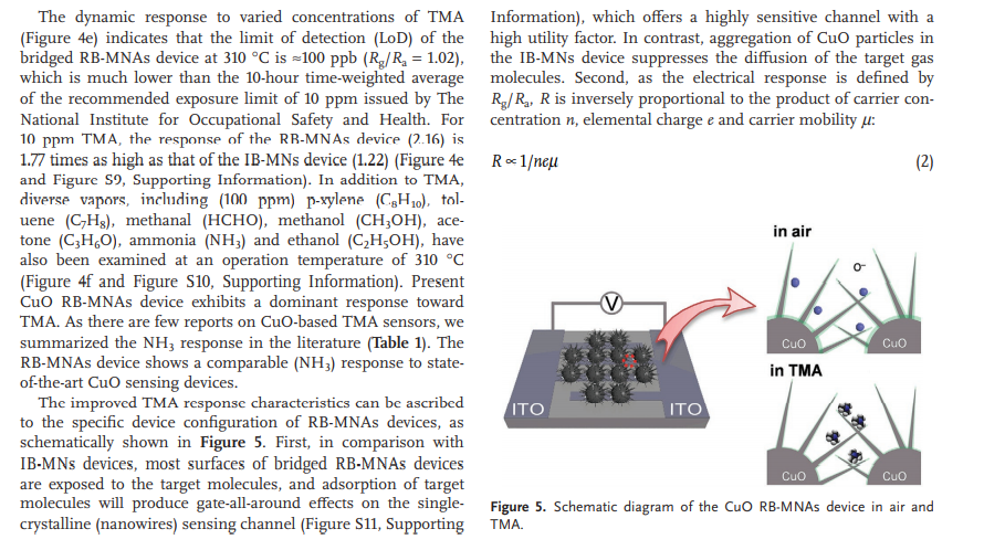
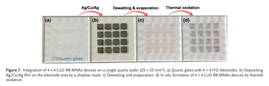
Device fabrication/integration is a longstanding challenge issue for the practical application of metal oxide nanowires with distinctive physiochemical and unique quasi-1D geometric properties.[1–3] In comparison with conventional planar nanowire devices, in which postsynthesis alignment (Langmuir–Blodgett technique,[4] contact printing,[5] and blow bubble,[6] etc.) is first employed and then electrodes are deposited, by directly growing nanowires on the selected area of solid substrates with bottom electrodes, when the tips of nanowires growing on the counter electrodes encompass each other and form stable junctions, a “bridged” nanowire device could be formed (at a large scale) in an in situ manner.[7–10] Apart from the superior benefits of facile integration of nanowire devices, bridged nanowire devices outperform conventional planar nanowire devices in several aspects. First, in situ growth ensures good electrical contact between the nanowires and the underlying electrode,[11] which plays an essential role in the performance of diverse microelectronic devices, including sensors,[12] photodetectors,[13] field emitters,[14] and energy storage devices.[15] Second, a nonplanar (or suspended) configuration not only avoids carrier scattering at the nanowire/substrate interface (leading to increased mobility)[16] but also offers a maximal exposure surface for analyte molecule adsorption (acting as a gate-all-around effect) and thus offers an additional avenue for designing highly sensitive sensors with ultralow power consumption.[7,11,17,18] As an important p-type oxide with versatile properties, CuO nanowires have promising applications in molecular sensors for harmful vapor monitoring,[19–23] photodetectors,[24] field emitting devices,[25] energy storage devices,[26] etc. Previous studies indicate that the number and density of bridged nanowires play an important role in the device performance (i.e., response and power consumption of gas sensors),[7,27] therefore, a rational synthesis methodology is essential for constructing high-performance devices. Though thermal oxidation of Cu (powder, foil, wire, film, etc.) offers a simple and catalyst-free method[28,29] for anisotropic growth of CuO nanowires, driven by oxidation induced strain between the CuO/Cu2O interfaces, as well as the fast outer diffusivity of Cu ions across the CuO/ Cu2O/Cu interfaces[29,30] and thermal oxidation of Cu powder or sputtered (patterned) Cu film dispersed/deposited onto the electrode substrate enabling the formation of bridged nanowires,[8,19] weak adhesion (due to thermal oxidation induced strain),[31] poor uniformity and uncontrolled electrical pathways hinder their promising applications. In this work, a novel methodology based on dewetting of patterned Cu films to create ordered Cu microhemisphere arrays was reported. Ag layer was proposed as a sacrificial layer to assist the dewetting of Ag/Cu/Ag films into microhemispheres at a relatively low temperature of 850 °C. Sacrificial Ag could be readily removed by vacuum evaporation due to the higher vapor pressure of Ag than Cu. In comparison with previously reported Cu powder or Cu film devices, Ag-assisted dewetting significantly shrinks the contact area of Cu/substrate to ≈1–500 µm2 (depending on size), which allows effective release of the interfacial stress during thermal oxidation of Cu[31] and contributes to firm adhesion with the underlying substrate. In addition, the position and size of hemisphere Cu arrays could be readily controlled, which plays a vital role in manipulating the structural properties (diameter, length and bridging density of nanowires) of CuO nanowires grown by thermal oxidation on diverse insulator substrates with indium tin oxide (ITO) electrodes. The in situ formed regularly bridged CuO microhemisphere nanowire arrays (RB-MNAs) devices exhibit much higher gas molecule and light responses than irregularly bridged microsphere nanowires (IB-MNs) devices, fabricated by thermal oxidation of Cu powder dispersed on ITO electrode substrates. For example, the electrical response (toward 100 ppm trimethylamine, TMA) of the RB-MNAs device is 2.8 times as high as that of the IB-MNs device at an operation temperature of 310 °C. The on/off current ratio toward (15.6 mW cm−2 ) 810 nm of the RB-MNAs device is 1.5 times as high as that of the IB-MNs device. Finally, 4 × 4 RB-MNAs devices were integrated onto a transparent ITO/quartz wafer, demonstrating the potential of the present methodology for the mass production of bridged CuO nanowire devices for future applications.
2. Results and Discussion
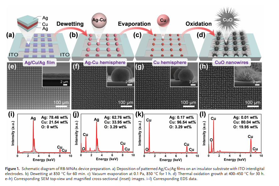
Although dewetting of uniform patterned metal films offers an approach to obtain homogeneous metal micro/nanoparticle arrays,[32,33] dewetting of patterned Cu films (prepared by using Ni shadow masks, the geometric parameters are listed in Table S1, Supporting Information) fails even at a high temperature of 850 °C. The high melting point of Cu (1085 °C) probably hinders the shrinking of the patterned Cu film at 850 °C (Figure S1, Supporting Information). Binary Cu-metal phase diagrams indicate that CuAg alloy (with 71.9 wt% Ag) possesses a low melting temperature of 779 °C,[34] which suggests that alloying with Ag may facilitate the dewetting of Cu film. Moreover, as the vapor pressure of Ag is much higher than that of Cu, Ag may be removed by appropriate thermal evaporation. Inspired by the abovementioned analysis, the patterned Cu film was sandwiched between the top and bottom Ag sacrificial layers (Ag/Cu/Ag) on a SiO2/Si or quartz substrate coated by ITO interdigital electrode (Figure 1a,e). As expected, the Ag/Cu/Ag film (size of 10.5 µm, thickness of 1.2/1.2/1.2 µm, with a Ag weight ratio of ≈70%) could be dewetted into a hemisphere shape (inset of Figure 1f) via vacuum or inert gas atmosphere annealing in a tube furnace (to prevent oxidation of metals) at 850 °C (Figure 1b,f). A noticeable decrease in the diameter of hemispheres from 8.0 ± 0.3 µm (Figure S2a, Supporting Information) to 7.0 ± 0.3 µm (Figure S2b, Supporting Information) was observed after performing vacuum evaporation (850 °C, 0.1 Pa, 1 h) (Figure 1c,g and Figure S2, Supporting Information). Moreover, the appearance of a dark condensed metal film in the low-temperature zone of the quartz tube furnace infers the evaporation of Ag, because the vapor pressure of Ag (≈2.8 × 10⁻¹ Pa) is much higher than that of Cu (≈2.3 × 10⁻³ Pa) at 850 °C.[35] Thermal oxidation of ordered Cu microhemispheres at 400–450 °C allows the formation of ordered hierarchical CuO microhemisphere nanowires (Figure 1d,h). Specifically, when the nanowires grown from adjacent Cu spheres contact each other, a bridged nanowire device could be formed in an “in situ” manner. To monitor the variation of sacrificial Ag, energy dispersive spectrometry (EDS) analysis was performed (Figure 1i–l). Pristine Ag/Cu/Ag shows a higher Ag ratio (78.5 wt%) than the nominal ratio (70.3 wt%), as EDS is a surface analysis method that can only collect the generated X-ray signal in a region of ≈2 µm in depth depending on the atomic number,[36] which is less than the thickness of the Ag/ Cu/Ag film (≈3.6 µm) in Figure 1e. The substantial decrease in the Ag component in the CuAg alloy from 62.7 wt% (Figure 1j) to a negligible 0.2 wt% (Figure 1k) via vacuum evaporation suggests that most of the sacrificial Ag was evaporated. Appearance of O signal in the dewetted CuAg and Cu hemispheres (Figure 1j,k) may arise from trace oxidization by remaining oxygen in the vacuum (≈0.1 Pa) tube furnace during dewetting and evaporation process. Moreover, the tiny variation in Cu volume from the initial Cu film (Figure 1e) to the hemisphere (Figure 1g) infers that Cu was maintained during the dewetting and evaporation process. The use of a Ag sacrificiallayer allows the fabrication of ordered Cu microhemisphere arrays (Figure 1c,g) on a solid substrate and further obtains ordered hierarchical CuO microhemisphere nanowire arrays (Figure 1d,h).


以上论文信息不完整 感谢中科大的孟老师对微型探针台的反馈!需要详细的文献,请到中科院一区 影响因子12 感谢所有的科研奉献者辛劳的付出。

 当前位置:
当前位置: